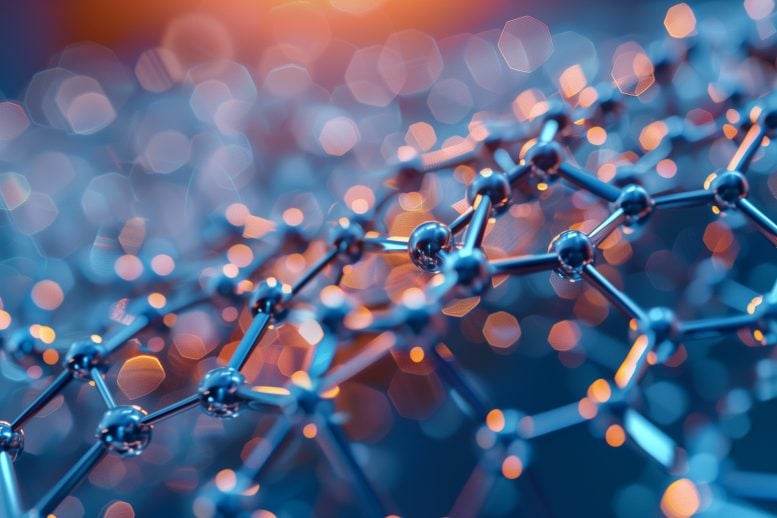
The researchers created half-tungsten carbide nanosheets that expand in the opposite direction of stretching, increasing their size by 40%. This breakthrough through plasma physics could lead to new applications in strain-sensitive technologies and stretchable electronics. (Artist’s concept). Image source: SciTechDaily.com
It is a common practice to stretch a balloon to make it easier to inflate. As the balloon stretches, the lateral width shrinks to the size of the rope.PhD student Noah Stocek collaborated with Western University physicist Giovanni Fanchini to develop a new nanomaterial that demonstrates the opposite of this phenomenon.
Stocek and Fanchini, working at Interface Science Western, home to the Tandetron accelerator facility, formulated two-dimensional nanosheets of half-tungsten carbide (or W2C, a compound containing equal amounts of tungsten and carbon atoms) that, when stretched in one direction, vertically Expands in response to applied force. This structural design is called auxetic.
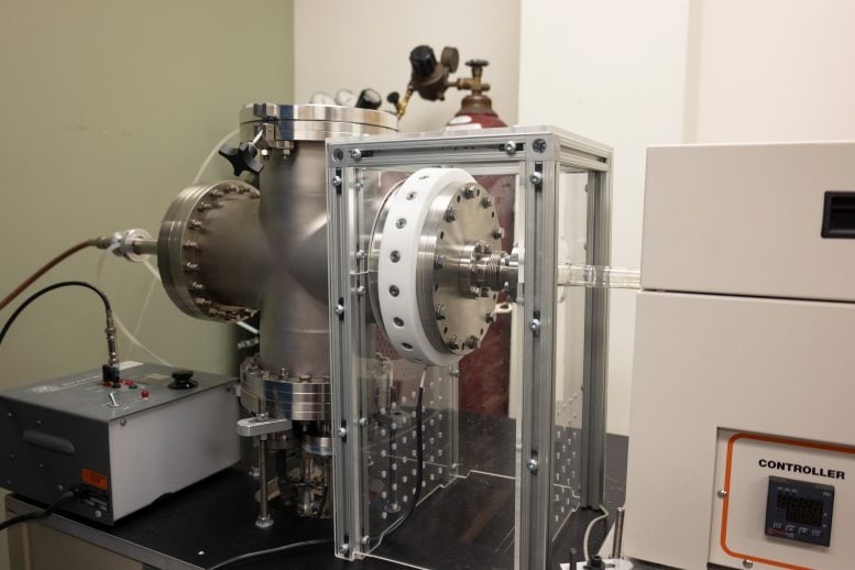
Remote plasma vapor deposition instrument designed by Fanchini Lab.Photo credit: Mitch Zimmer/Western Science
The trick is that the structure of the nanosheets themselves is not flat.The atoms in the sheet are made up of repeating units of two tungsten atoms for each carbon atom. atom, they are arranged like the uneven surface of an egg carton. When tension is applied to the elastic nanosheet in one direction, as the dimple flattens, it expands in another dimension.
Prior to this innovation, only one material was reported to expand by 10% per unit length in this counterintuitive way. Western-designed semi-tungsten carbide nanosheets can expand up to 40%, setting a new world record.
“We specifically want to create a two-dimensional nanomaterial using half-tungsten carbide,” Stocheck said. “In 2018, theorists predicted that it might exhibit this behavior brilliantly, but despite extensive attempts by research groups around the world, no one was able to develop it.”
It was impossible to construct new semi-tungsten carbide nanomaterials using chemical methods, so Stocek and Fanchini relied on plasma Physically form a single atomic layer. Plasma is composed of electrically charged atomic particles and is the fourth state of matter (solid, liquid, and gas). Plasmas can be observed in nature in the Aurora Borealis, or Aurora Borealis, and in the solar corona during recent solar eclipses. It is also used in neon lights, fluorescent tubes and flat screen televisions.
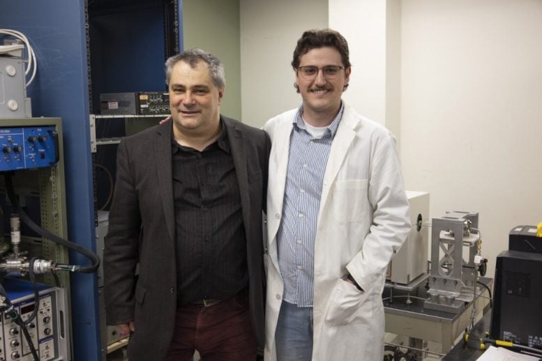
Giovanni Fanchini and Noah Stocheck.Photo credit: Mitch Zimmer/Western Science
Typically, the instruments used to make 2D nanomaterials are special furnaces in which gases are heated to a high enough temperature to chemically react and form the desired substances. This approach simply doesn’t work because any chemical reaction (the most common process) would produce a different product than the desired nanomaterial.
“This is where most researchers who tried to get this material before us got stuck, so we had to pivot,” Fanchini said.
Rather than heating a gas made of tungsten and carbon atoms in a furnace, which creates neutral particles like a solid, liquid or gas, Stocek and Fanchini designed a new custom-made instrument that can create a plasma, a plasma The body is made up of electrically charged particles.
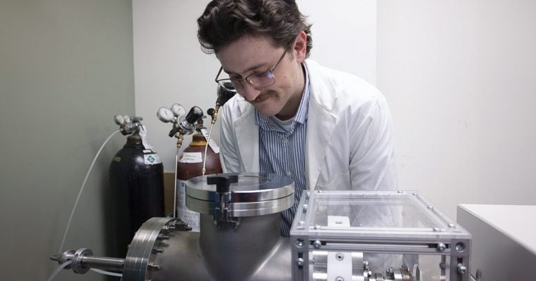
Western University doctoral student Noah Stocek uses a custom instrument he designed with Giovanni Fanchini that produces record-breaking amounts of two-dimensional nanomaterials.Photo credit: Mitch Zimmer/Western Science
stretch goals
There are countless possible applications for these W2C nanosheets, starting with new strain gauges. These commercial gauges are the standard way to measure expansion and tension in everything from airplane wings to home pipes.
“Imagine if you wanted to know if the pipes in your home were warped and at risk of breaking at some point. You could attach sensors to pipes made of this two-dimensional nanomaterial and use a computer to monitor the passage of Its current. If the current rises, that means the pipe is expanding and at risk of rupture,” Stocheck said.
The fact that new nanomaterials become more conductive opens the door to endless possibilities for things like sensors or any device that detects environmental events or changes and sends the information to other electronic devices. Another application is embedding the material into stretchable electronics, such as wearable technology, so that they are more conductive.
“Typically, strain gauges rely on the fact that when you stretch a material, it becomes thinner and changes the conductivity of the material to carry the current,” Fanchini said. “With this new nanomaterial , this will no longer be the case.”
Reference: “Giant auxetic behavior in remote plasma synthesized few-layer tungsten semicarbide” by Noah B. Stocek, Farman Ullah and Giovanni Fanchini, April 8, 2024 material vision.
DOI: 10.1039/D3MH02193A
Funding: NSERC DG, Ontario Graduate Scholarship, NSERC Strategic Partnership Grant, NSERC RTI, Canada Foundation for Innovation, Natural Sciences and Engineering Research Council of Canada
#Scientists #discover #nanomaterials #counterintuitive #expansion #properties
Image Source : scitechdaily.com